
News
Do You Know HDI PCB Fabrication Basics
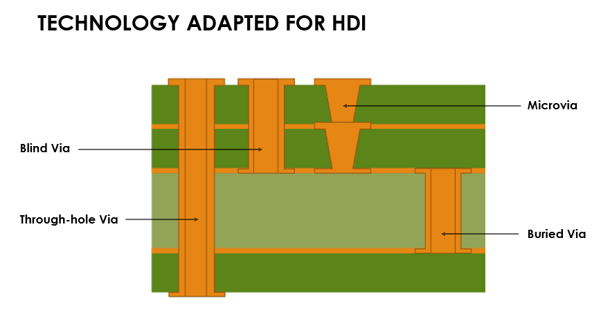
High Density Interconnect (HDI) Printed Circuit Board (PCB) actually started in 1980, when researchers investigating ways to reduce the size of vias. With years rapid development of HDI boards, sequential build-up (SBU) technology is most widely used method for HDI manufacturing process, please refer to below figure. But do you know HDI PCB fabrication basics?
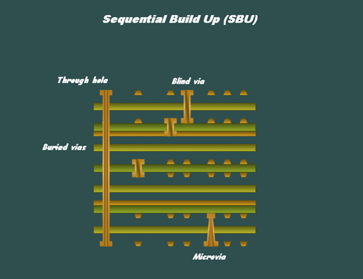
Sequential Buil-up (SBU) Technology
From this figure, there are three basic elements, which are Dielectric format, via formation and metallization methods. The HDI board manufacturing process for each microvia technology begins with a base core, which may be a simple double-sided board carrying power and ground planes or a multilayer board carrying some signal pattern in addition to power and ground planes. The core usually has plated through-holes (PTHs). These PTHs become blind via holes. Such a core is often called an active core.Dielectric and Insulators
An overview of the dielectric and applied conductive materials used in microvia fabrication are covered in IPC-4104A standard. Some of these dielectrics can be used in both chip packaging and HDI PCB applications. Cross-references are made to the relevant material specifications of the IPC/JPCA-4104 specification for HDI and microvia materials.
Material selection needs to answer these questions:
Will the dielectric use chemistry compatible with current chemistry used by core substrate material?
Will the dielectric provide adequate and reliable dielectric spacing between metal layers?
Will it meet thermal needs?
Will the dielectric provide a desirable “high Tg” for wire bonding and rework?
With it survive thermal shock with multiple SBU layers (i.e. solder floats, accelerated thermal cycles, multiple reflows)?
Will it have plateable, reliable microvias (that is, will it have latitude to ensure good plating to the bottom of the via)?
There are nine different general dielectric materials used in HDI substrates. IPC slash sheets like IPC-4101B and IPC-4104A cover many of these, but many are not yet specified by IPC standards. The materials are:
Photosensitive Liquid Dielectrics
Photosensitive Dry Film Dielectrics
Polyimide Flexible Film
Thermal cured Liquid Dielectric
Resin Coated Copper Foil (RCC), dual-layer and reinforced
Conventional FR4 Cores and Prepregs
New spread-glass laser-drillable (LD) Prepregs
Thermoplastics
Interconnect Via Formation
This section discusses processes that employ various drilling via-hole formation techniques. Through-via drilling is possible below 0.20mm (8mil), but cost and practically discourage this. Below 0.20mm (8mil), laser and other via-formation processes are most cost-effective. There are many different methods of forming the Interstitial Via Hole (IVHs) used in HDI PCB manufacturing processes. Laser drilling is the most prominent. These different methods of via formation have some limits on the minimum size of the vias they form, as well a significant difference in rate of via formation.
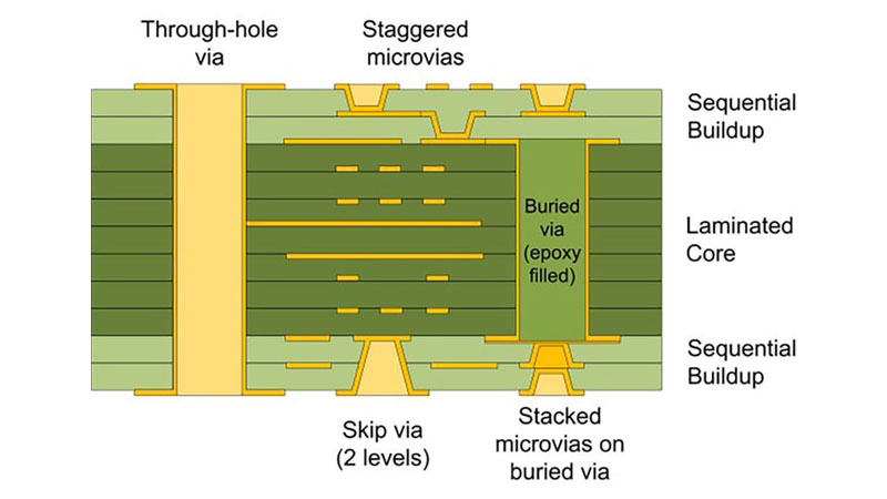
In HDI board fabrication, the small vias can be mechanically drilled by either controlled-depth, figure (a), or sequential lamination, figure (b).
Mechanical Drilling
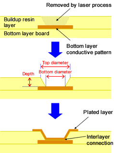
The oldest technique for blind and buried via formation is mechanical drilling and sequential lamination, as seen in figure (a) and (b) posted above. Progress has been made in both small drill-bit manufacturing and high-speed mechanical drilling to allow this technique to be used in some circumstances. The figure below describes creating the blind-via in a PCB panel is normally done with laser technology but mass via processes like chemical etching, plasma or photo-dielectrics have also been used.
Laser Via Technology
Laser Via processing is by far the most popular microvia hole formation process. But it is not the fastest via formation process. The chemical etching of small vias is the fastest, with an estimated rate of 8,000 to 1,2000 vias per second. This is also true of plasma via formation and photovia formation (Figure above). These are all mass-via-formation processes. Laser drilling is one of the oldest microvia generation techniques. The wavelengths for laser energy are in the infared and ultraviolet region. Laser drilling requires programming the beam influence size and energy. High-fluence beams can cut metal and glass, whereas low-fluence beams cleanly remove organics but leave metals undamaged. A beam spot size as small as approximately 20?m (<1mil) is used for high-fluence beams and about 100?m (4mil) to 350?m (14mil) for low-fluence beams.
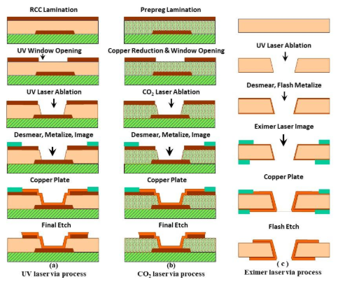
Most laser processes utilize either CO2 or UV lasers since they are the most readily available and economical lasers. When using a CO2 laser to produce vias in epoxy laminates, the copper must be removed above the area to be ablated (see figure below). The CO2 laser is primarily used for laminates not supported by glass. This includes unsupported laminates such as flexible polyimide and resin-coated copper (RCC) foil and laminates reinforced with alternative materials such as aramid fibers. The modified TEA CO2 (Transversely Excited Atmospheric) lasers are specifically created to laze through glass fibers using 9,000nm wavelength and higher peak power.
However, there are many variations. For purpose of drilling microvia holes, there are five laser systems in HDI PCB manufacturing industry: UV/Eximer, UV/Yag laser, CO2 laser, Yag/CO2, and CO2/TCO2 combinations. There are also many dielectric materials: RCC, resin only (dry film or liquid resin), and reinforced prepreg. Therefor, the number of ways to make microvia holes by laser systems is driven by the permutation of five laser systems and these dielectric materials, as seen in figure.
Higher power lasers (i.e. Ultra Voilet-UV) can remove glass and copper and can therefor be used with conventional laminates, but are typically slower when going through copper and glass fibers. There are several factors to consider in laser via processing: position accuracy of lased holes) microvia holes), uneven diameters of holes, and dimensional change of the panel after curing dielectric, dimensional change of the panel due to temperature and humidity variations, alignment accuracy of the photo-exposure machine, unstable nature of negative artwork, and so on. These should be carefully monitored and are important for all microvia hole processes.
Method of Metallization
The last process is metallization of the vias. There are four different methods of metallizing the IVHs used in HDI processes. The methods are:
Conventional Electroless and Electroplating Copper
Conventional Conductive Graphite or other Polymers
Fully and Semi-Additive Electroless Copper
Conductive Pastes or Inks (below figure h and figure i)
The laser is the most used method of production of microvias to be filled with a conductive paste. Lasers are capable of ablating dielectric material and stopping when intercepting the copper circuitry, so they are ideally suited for creation of depth-controlled blind vias. Figure below shows these two major microvia processes.
Two of the most popular processes for microvia hole metalization is with conductive polymers; f. The BBiT process screens a conductive silver paste on copper foil and laminates it into the 2-sided core; g. Various conductive pastes are screened into laser-drilled holes in the b-stage dielectric and then laminated with copper foil into the core.